This study investigates the airflow distribution and thermal behavior within a wafer burn-in test system using CFD analysis. The results provide guidance for improving temperature uniformity and system reliability
1. What Is a Wafer Burn-In Test System?
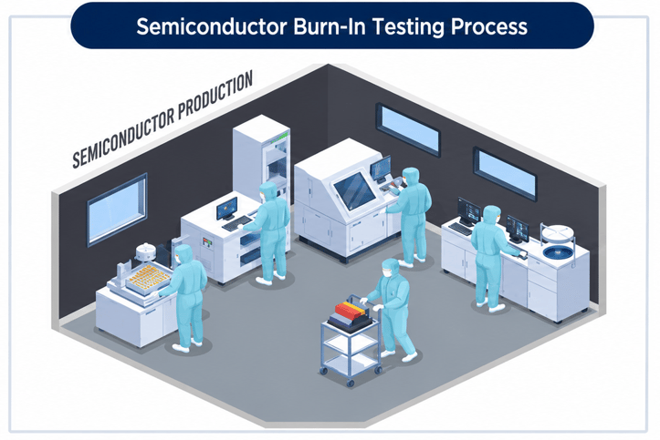
The Wafer Burn-In Test System is applied during the final stage of wafer processing, specifically in the wafer inspection and reliability verification process. Burn-in testing is a procedure in which semiconductor devices are subjected to elevated temperatures and higher-than-normal operating voltages before shipment to customers. This accelerated stress environment is used to identify latent defects and evaluate product reliability at an early stage.
As semiconductor devices become increasingly miniaturized, highly integrated, and high-speed, post production failures can significantly increase manufacturing costs. To mitigate this risk, burn-in testing is performed to eliminate early-life failures and improve product reliability before packaging and shipment .
2. Why Is the Wafer Burn-In Process Important?
Semiconductor devices often exhibit a relatively high failure rate during the early stage of operation, while long-term use typically results in a much lower failure rate. Therefore, removing these early failures is essential for improving overall product reliability.
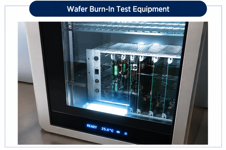
The primary objective of a wafer burn-in system is to perform accelerated life testing that screens out defective devices before shipment, thereby ensuring the reliability of the final product. Another key challenge is introducing new products while minimizing investment costs and maximizing production yield. This benefits semiconductor manufacturers, equipment suppliers, and end users alike.
By performing burn-in testing at the wafer level rather than after packaging, manufacturers can improve both reliability and yield while reducing overall testing costs.
To accommodate various packaging types and operating environments, CFD (Computational Fluid Dynamics) analysis can be used to optimize thermal and flow performance, enabling improved product characteristics within minimum development time and cost.
Before semiconductor products are delivered to customers, they are exposed to elevated temperatures and voltages higher than normal operating conditions to identify potential defects and verify reliability. CFD analysis can be utilized to optimize equipment design, improve testing efficiency, and reduce the occurrence of early-life failures, ultimately enhancing product reliability .
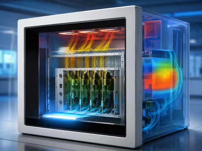
03. What Should Be Considered for Thermal Fluid Dynamics Analysis of Test Equipment?
Accurate thermal fluid dynamics analysis requires proper definition of operating conditions, including airflow rate, pressure, temperature, and internal heat generation. Since test equipment operates under elevated temperatures, realistic thermal boundary conditions are essential.
Airflow uniformity within the chamber should be evaluated to identify recirculation zones and ensure consistent cooling performance. Temperature distribution across test boards or wafers must also be verified to prevent hot spots and maintain reliable test conditions.
In addition, pressure loss caused by internal structures should be minimized to improve system efficiency. CFD analysis enables optimization of airflow and temperature uniformity, helping improve product reliability while reducing development time and cost.
list view